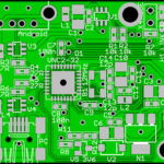
Downloads
- AndropodInterface Software-Tutorial (en)
- AndropodInterface Software-Tutorial (de)
- AndropodInterface Schematics V1.2
- AndropodInterface Schematics V3.3
- AndropodInterface Hardware V1.2
- AndropodInterface Hardware V3.3
- AndropodInterface V0.9 beta
- AndropodInterface Logos
What is the AndropodInterface?
It works without any modifcation of the Android device – just with your unmodified Android!
What makes the AndropodInterface so special?
What is the AndropodInterface for?
You can use it for example in robots, drones, phone docks, gadgets or any project you can think of.
What allows me the AndropodInterface to do?
Ever wanted to be able to get GPS data or accelerometer values in your project?
Ever wanted to have a huge color display with touchscreen on your project?Then the AndropodInterface is the right thing for you!
The AndropodInterface gives you the possibility to harvest all the functionality of your mobile phone for your projects!
You want to read more about the Andropod Interface?
You can download the article in multiple languages at Elektor:
Andropod (1) – Elektor UK, USA, Canada (English)
Andropod (1) – Elektor Germany (German)
Andropod (1) – Elektor Spain (Spanish)
Andropod (1) – Elektor Netherlands (Netherlands)
Sounds good – but expensive, right?
The basic hardware for it will start at about 25€ / 35$ and is widely available at Digikey / Farnell / Newark / RS!
If you build your own PCB the additional hardware cost will be as low as about 3€ / 5$!If you are looking for a completely tested and plug an play solution go for the Andropod Interface that was built together with electronic magazine Elektor. Visit their shop at:
http://www.elektor.com/products/kits-modules/modules/110405-91-andropod.2052293.lynkx
See it in action!
Getting the hardware:
I don’t care about how it works, i want to use it!
Elektor Shop
I want to modify the firmware myself
I want it small and modify the hardware to fit my needs!
WRITING the Android app
try
{
     //Create new server
     ServerSocket socket = new ServerSocket(1337);

     //Wait until the andropodInterface is connected
     Socket andropodInterface = socket.accept();

     //Open streams
     PrintReader in = new BufferedReader(new InputStreamReader(andropodInterface.getInputStream()));
     PrintWriter out = new PrintWriter(andropodInterface.getOutputStream(), true);

    //Write what you want to write
    out.println("Hello Androdpod!");

     //Read what you want to read ;-)
    string message = in.readln();
}
catch (IOException e)
{
    //Something went really wrong
}
Connecting
- Configure the Andropod Interface with your PC
Install the Andropod Configuration Software on your PC, switch the Andropod Interface to “Configure Mode” (you will find an image with the correct jumper settings in the software) and connect it to your PC using a standard Micro USB cable. Then you can configure the baudrate an other settings as required by your application. Save all changes and you are ready to go. - Connect it to your robot, drone, gadget or other Hardware
Use four simple wires, two for the supply voltage +5V, GND and the two serial RX and TX wires.
The AndropodInterface needs 5V at around 550mA, in order to be able to charge the attached Android phone (if you disable that Android charges the phone when connected to USB, that the power consumption will be down to a few mA)
Now one LED on the Andropod Interface should light up - Enable the USB Debugging in your Android phone
This is needed in order to make the magic hapen – don’t forget to do that! - Connect your Phone to the AndropodInterface
Now the second LED on the AndropodInterface should start blinking, and the phone should tell you that USB debugging is connected - Start your application on the Android phone!
Now the second LED should go from blinking to permanent on - Your hardware is now an Andropod – have fun with it – put a Andropod logo on your hardware and send us pictures =)
HOW IT WORKS
First considerations
Embedded systems constantly evolve and developing state-of-the art systems for educational purposes is a very time consuming and expensive process. In order to provide the highest possible processing power along with sophisticated communication interfaces like Wireless Lan, HSDPA and Bluetooth to embedded projects using cheap and well tested high-end smart phones would be the best solution.
Currently the Smartphone market is split into a few different segments – the three major OSes are currently the Blackberry OS featured on most of the RIM (Research In Motion) devices, the iOS devices that is used on most Apple mobile devices and finally Google’s Open Source Android OS that is currently powering several hundred devices from multiple manufacturers.
When using Smartphones on for example Robotic projects the cost, the availability and the openness and power of the software framework are the key factors. Considering these factors the Open Source Android platform seems to meet the demands at best. The devices are really cheap (from around 100€ or less) and available from a variety of different hard manufacturers and the software is completely open, thus it’s an open source project distributed partially under the GNU GPL and the Apache Licensing model.
The big problem is how to communicate with Android-based mobile devices from custom embedded hardware in order to control robotics or for example sensor data. The general problem in this concern is that most Android devices (contrary to Apple devices) feature only one USB-OTG in port (a dual role – host or device – USB 2.0 port).
Main objective of this document is to discuss the mechanisms to interface Android devices with any simple serial (TTL-Serial, I²C, SPI) or parallel bus.
Another – on the first sight – more complex solution is to use the Android device’s USB controller in device mode, what requires the custom hardware to feature a more complex USB host port.
Using a host port simplifies the work that needs to be done on the Android smart phone itself what should – in the end – lead to a plug and play solution for all Android devices.
In order to ensure the plug and play experience that data exchange needs to be done over one of the following USB device classes already implemented in Android.
- USB mass storage device class (g_storage)
- USB Ethernet device class (g_ether)
- Android ADB debug interface (adb)
In general only the adb and the g_storage interface are implemented across all Android devices – the g_ether device made it as “USB Thethering” to Android 2.1 and might be problematic to use on devices that have no Baseband – like the Archos Tablets, or devices imported from the US – cell phone carriers tend to disable this feature to reduce the overall cell network usage and therefore increase net stability.
The g_storage interface:
The g_ether interface:
The ADB interface:
The discrete implementation
After considering everything learned in the previous chapter this chapter describes the implementation of a black-box USB host for Android device to serial solution based on the Android Debug interface.
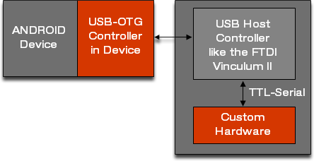
As USB host a Vinculum II from FTDI is used. The VNCII is highly optimised USB controller that features two dual role USB ports in combination with a 16bit core with Harvard architecture, 256kb of flash memory and 16kb of RAM along with several communication interfaces (UART, SPI, 8-bit FIFO, …). The Vinculum II is priced at about 3.50€ for low quantity orders (10 part or more), what is quite cheap considering the prices of “normal” USB serial converters like the CP2102(2,56€) or the FT232 (5,10€).
FTDI provides a complete IDE with it’s VOS (Vinculum OS) that includes all necessary libraries for USB development, suitable evaluation kits start at 30€ and a fully featured debugger / programmer will cost around 20€ – so developing hardware with the VNC2 is really cheap and quite easy.
The Android Debug Bridge
The Android Debug Bridge is as its name says just a bridge between the debugging PC and the Android device. It allows tunneling TCP ports (for example to attach to debugging session to the gdb server) as well as remote access to the system shell and file exchange between the client and the host system.
Generally the ADB “driver” itself is always implemented in userspace (in Linux, Windows and Mac). The ADB software directly accesses the USB FIFOs of the USB device to be more specific the ADB uses only two FIFOs one incoming and one outgoing endpoint. The endpoints are bulk endpoints so no the data integrity is ensured by low-level USB layers. Considering all these facts the ADB USB layer is nothing more than a high speed serial connection that provides error handling and correction mechanisms.
The protocol on top of the USB connection is a simple as possible:
struct amessage {
unsigned command; /* command identifier constant */
unsigned arg0; /* first argument */
unsigned arg1; /* second argument */
unsigned data_length; /* length of payload (0 is allowed) */
unsigned data_check; /* checksum of data payload */
unsigned magic; /* command ^ 0xffffffff */
};
…
amessage msg;
unsigned char data[MAX_PAYLOAD];
…
The structure and the data (limited to a maximum packet size of 4kb) is sent over the USB connection. The 32 bit data fields are converted to little endian byte order.
HARDWARE
The hardware implementation is in general quite simple and the block diagram of an example system using the VNC2 should look like the following figure shows:
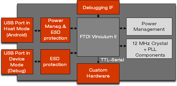
Everything explained
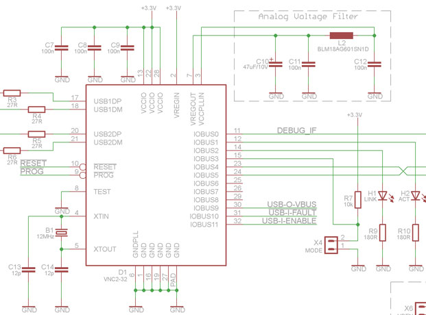
The processor
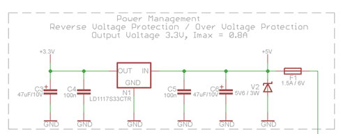
The Power Managment
USB Overcurrent protection
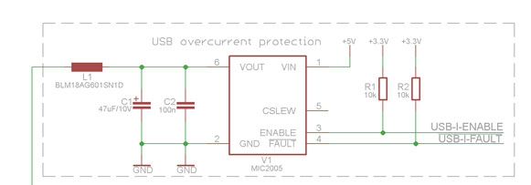
The output contains a standard LC network used to stabilize the output voltage and minimize interference coming from the USB connector.
USB Connectors
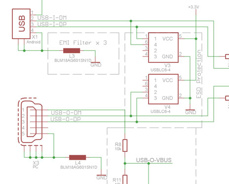
In order to minimize EMI noise effects small inductors have been installed on all USB power lines.
To provide maximum ESD performance USBLC6-4 from ST semiconductor has been installed – basically these ICs are diode networks to protect the circuitry from high voltage spikes (kV area). Normally one IC can be used to protect both USB connections –but due to layout considerations two ICs have been used.
VBus sensing
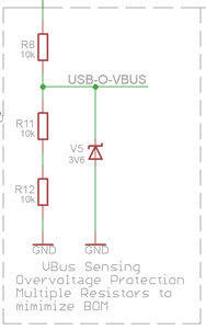
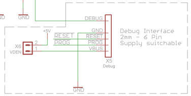
Debug interface
Serial connector
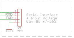 The 4 pin connector used for serial communication with the embedded hardware contains only the basic RX, TX and ground connection – to minimize complexity no hardware handshake has been implemented. The serial connector is also the main source for the system power – the system should supply 5V at 750mA to the board. The voltage must not be without a range of +/-10% around 5V – to be fully USB 2.0 compliant the voltage must not be without a range of 4.4V to 5.25V. As again this interface is considered to be “safe” and only a in system connection – no ESD precautions have been made.
FIRMWARE
General
The tricky part of the AndropodInterface is definitively the firmware that needs to be programmed into the microprocessor.
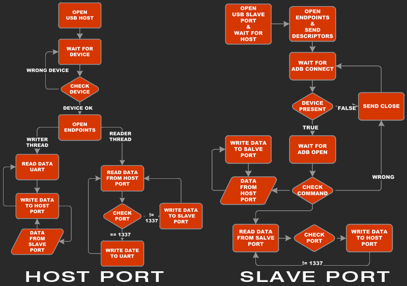
A very simplified overview over the firmware could look like the:
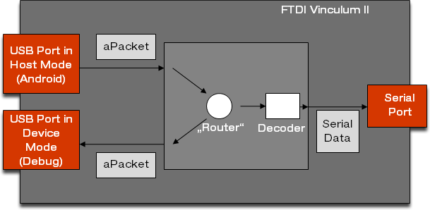
One of the USB ports is configured as slave, the other one is configured as host. All the data received from the host (the Android phone) and the slave (the PC) is read and sent to an internal packet “router”. This part of software analyzes all packets received form the slave and from the host and passes all packets under normal operation just from host to slave. If a packet contains information that it is sent to or from the TCP port 1337 the payload data is redirected to the serial port.
Working with the Vinculum
Basically the development with the Vinculum II plattform is quite easy for higher level application – but more complex for the simple things, like setting a port pin.
The Vinculum II IDE and toolchain has a very good driver system – which packs all device drivers into the same interface – each driver consists of the following functions:
- Open
- Read
- Write
- Ioctl
Generally the AndropodInterface needs a few drivers or has implemented the following driver:
- USB Slave driver
- Custom USB Slave driver
- USB Host driver
- Custom USB Host driver
- Serial Port driver
The Android Debug Bridge
The Android debug bridge is a really simple protocol – all the data is packed into packets that are up to 4096 bytes long and are of the following structure:
struct amessage {
unsigned command; /* command identifier constant */
unsigned arg0; /* first argument */
unsigned arg1; /* second argument */
unsigned data_length; /* length of payload (0 is allowed) */
unsigned data_check; /* checksum of data payload */
unsigned magic; /* command ^ 0xffffffff */
};
…
amessage msg;
unsigned char data[MAX_PAYLOAD];
…
Protocol description
The command id is the first byte transmitted in the header of a message, it contains one of the following commands:
- CONNECT (“CNXN” => 0x4e584e43)
“CONNECT(version, maxdata, “system-identity-string”)
The CONNECT message establishes the presence of a remote system.The version is used to ensure protocol compatibility and maxdata declares the maximum message body size that the remote system is willing to accept.Currently, version=0x01000000 and maxdata=4096Both sides send a CONNECT message when the connection between them is established. Until a CONNECT message is received no other messages may be sent. Any messages received before a CONNECT message MUST be ignored.If a CONNECT message is received with an unknown version or insufficiently large maxdata value, the connection with the other side must be closed.The system identity string should be “<systemtype>:<serialno>:<banner>” where systemtype is “bootloader”, “device”, or “host”, serialno is some kind of unique ID (or empty), and banner is a human-readable version or identifier string (informational only).” - Ready (“OKAY” => 0x59414b4f)“READY(local-id, remote-id, “”)
The READY message informs the recipient that the sender’s stream identified by local-id is ready for write messages and that it is connected to the recipient’s stream identified by remote-id.Neither the local-id nor the remote-id may be zero.A READY message containing a remote-id which does not map to an open stream on the recipient’s side is ignored. The stream may have been closed while this message was in-flight.The local-id is ignored on all but the first READY message (where it is used to establish the connection). Nonetheless, the local-id MUST not change on later READY messages sent to the same stream.” - Open (“OPEN” => 0x4e45504f)
‘”OPEN(local-id, 0, “destination”)
The OPEN message informs the recipient that the sender has a stream identified by local-id that it wishes to connect to the named destination in the message payload. The local-id may not be zero.The OPEN message MUST result in either a READY message indicating that the connection has been established (and identifying the other end) or a CLOSE message, indicating failure. An OPEN message also implies a READY message sent at the same time.Common destination naming conventions include:
* “tcp:<host>:<port>” – host may be omitted to indicate localhost
* “udp:<host>:<port>” – host may be omitted to indicate localhost
* “local-dgram:<identifier>”
* “local-stream:<identifier>”
* “shell” – local shell service
* “upload” – service for pushing files across (like aproto’s /sync)
* “fs-bridge” – FUSE protocol filesystem bridge” - Write (WRTE => 0x45545257)
“WRITE(0, remote-id, “data”)
The WRITE message sends data to the recipient’s stream identified by
remote-id. The payload MUST be <= maxdata in length.A WRITE message containing a remote-id which does not map to an open
stream on the recipient’s side is ignored. The stream may have been
closed while this message was in-flight.
A WRITE message may not be sent until a READY message is received.
Once a WRITE message is sent, an additional WRITE message may not be
sent until another READY message has been received. Recipients of
a WRITE message that is in violation of this requirement will CLOSE
the connection.” - Close(“CLSE” => 0x45534c43)“CLOSE(local-id, remote-id, “”)
The CLOSE message informs recipient that the connection between the sender’s stream (local-id) and the recipient’s stream (remote-id) is broken. The remote-id MUST not be zero, but the local-id MAY be zero if this CLOSE indicates a failed OPEN.A CLOSE message containing a remote-id which does not map to an open stream on the recipient’s side is ignored. The stream may have already been closed by the recipient while this message was in-flight.The recipient should not respond to a CLOSE message in any way. The recipient should cancel pending WRITEs or CLOSEs, but this is not a requirement, since they will be ignored.”
Note: The Information written italic is copied from the “protocol.txt” of the Windows / Linux ADB implementation.
An overview of the firmware
A closer look on the firmware unveils the following general structure of the firmware:
